While tower has great range of sensors, possibilities of controling something are very limited, so I ended up building own HW for everything I needed to control so far. I don’t really enjoy making own PCBs and especially 2-sided ones are pain to make. So I decided to design some universal PCBs covering most typical scenarios (at least for me) and get them manufactured professionally in small batch. Then I will just fit components I need for particular use case.
Scenario #1: PWM
My most typical use case is using PWM to control something. Apart from dimming LED stripes, it can be used to control fans or driving servos.
Features:
power 5-24V (up to 40V with AP1501 converter),
optional battery module (useful for sending messages in case of power outage),
option to connect battery analog signals to P0+P1 (original design) or P4+P5 (in case you want use P0+P1 as PWM outputs),
any combination of output connectors as long as they have 5.08 mm spaced pins with option to connect PWM, GND or VCC to any output pin,
correct handling of VDD_OFF and BAT_OFF signals,
ability to handle decent load (I guess most limiting are vias between ground and transistors, able to handle about 3A per output pair, eg. 3A if you connect VCC to next pin or 1.5A if you connect PWM or GND on both).
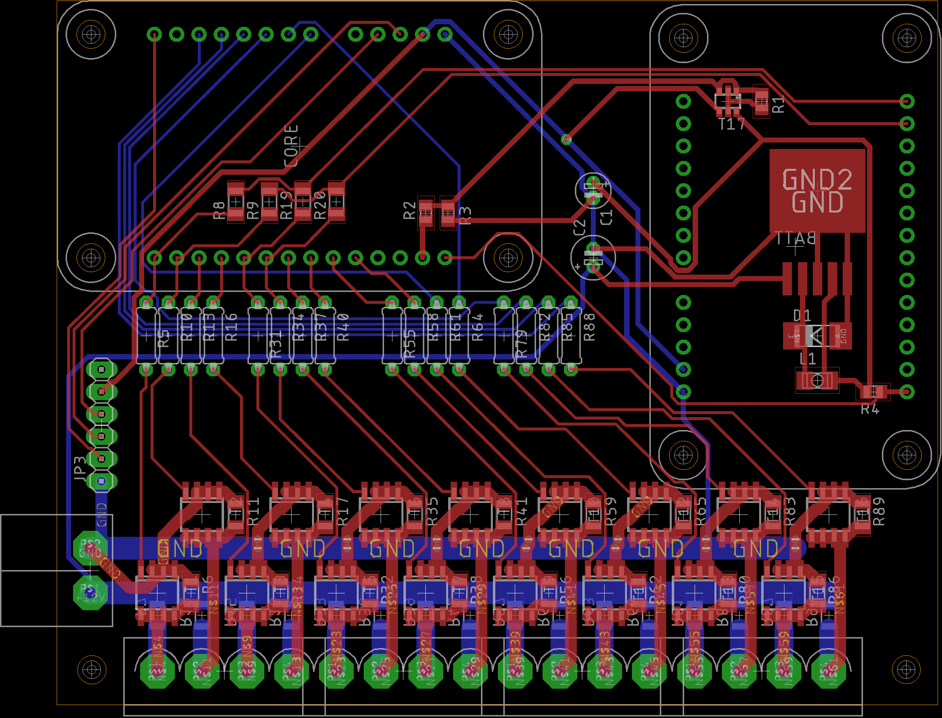
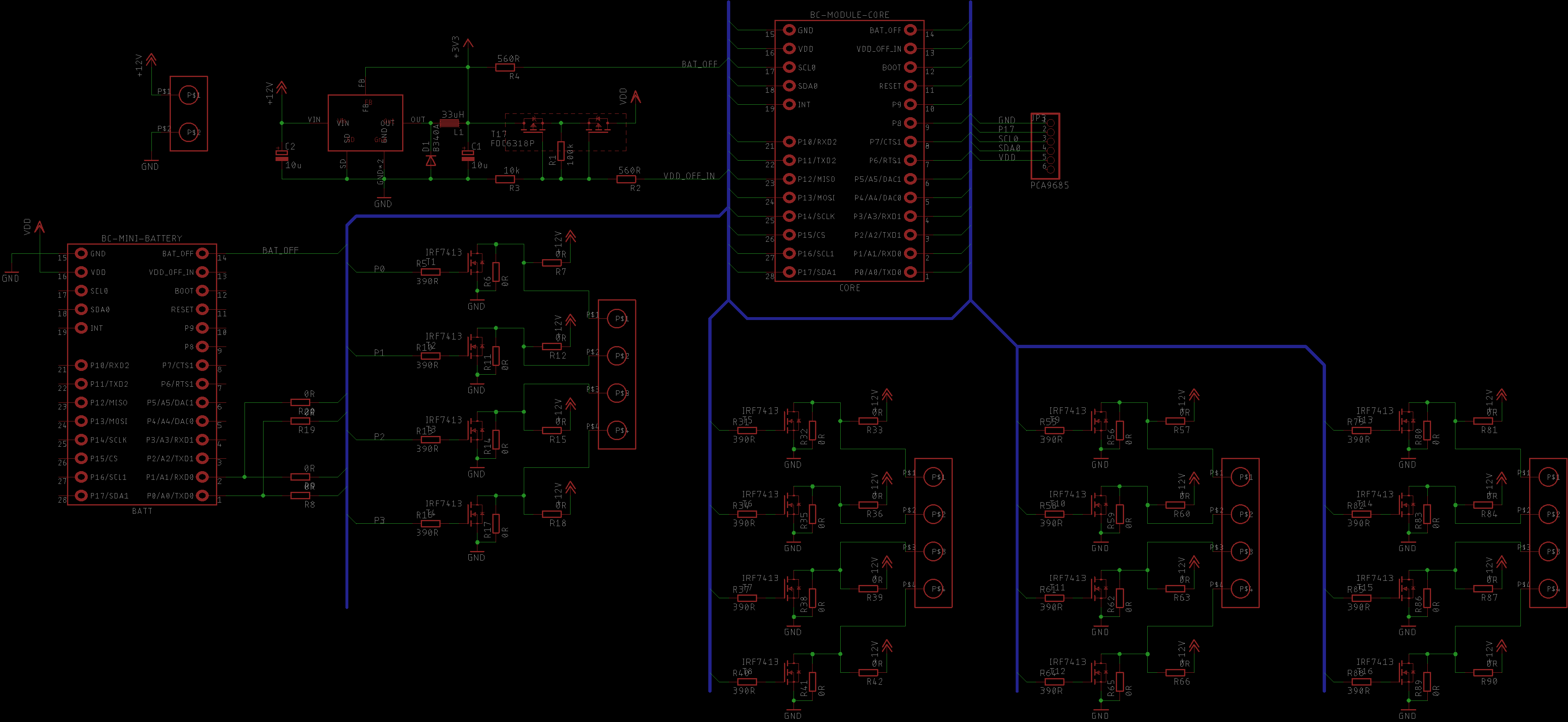
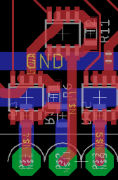
In schema, there are all components, even those mutually exclusive, so it might not make sense at first sight. Also, it might be necessary to place resistors diagonally if you need GND/VCC on output pin next to PWM (for example to have outputs PWM, +12V, PWM, +12V… you can place resistor from P1 to 3rd output). Not very nice, I know, but it will do the job
Any feedback is welcome, I’m not very experienced in HW design (I’m mostly SW guy) so there probably are some flaws . Power converter was taken from the AP1501 datasheet and VDD_OFF / BAT_OFF handling was taken from Hardwario power module (I wasn’t sure about some aspects, so I basically copied it 1:1).
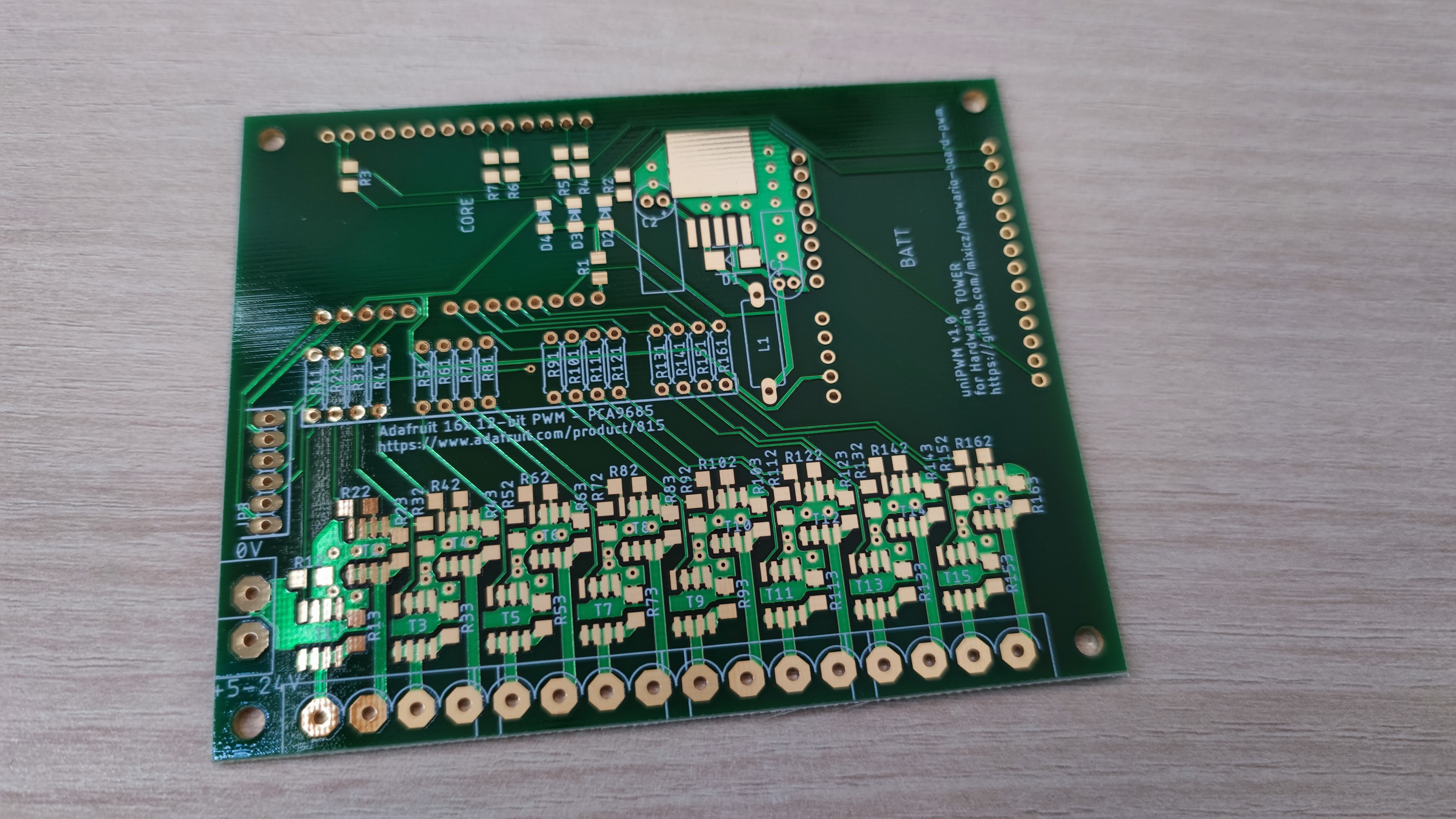
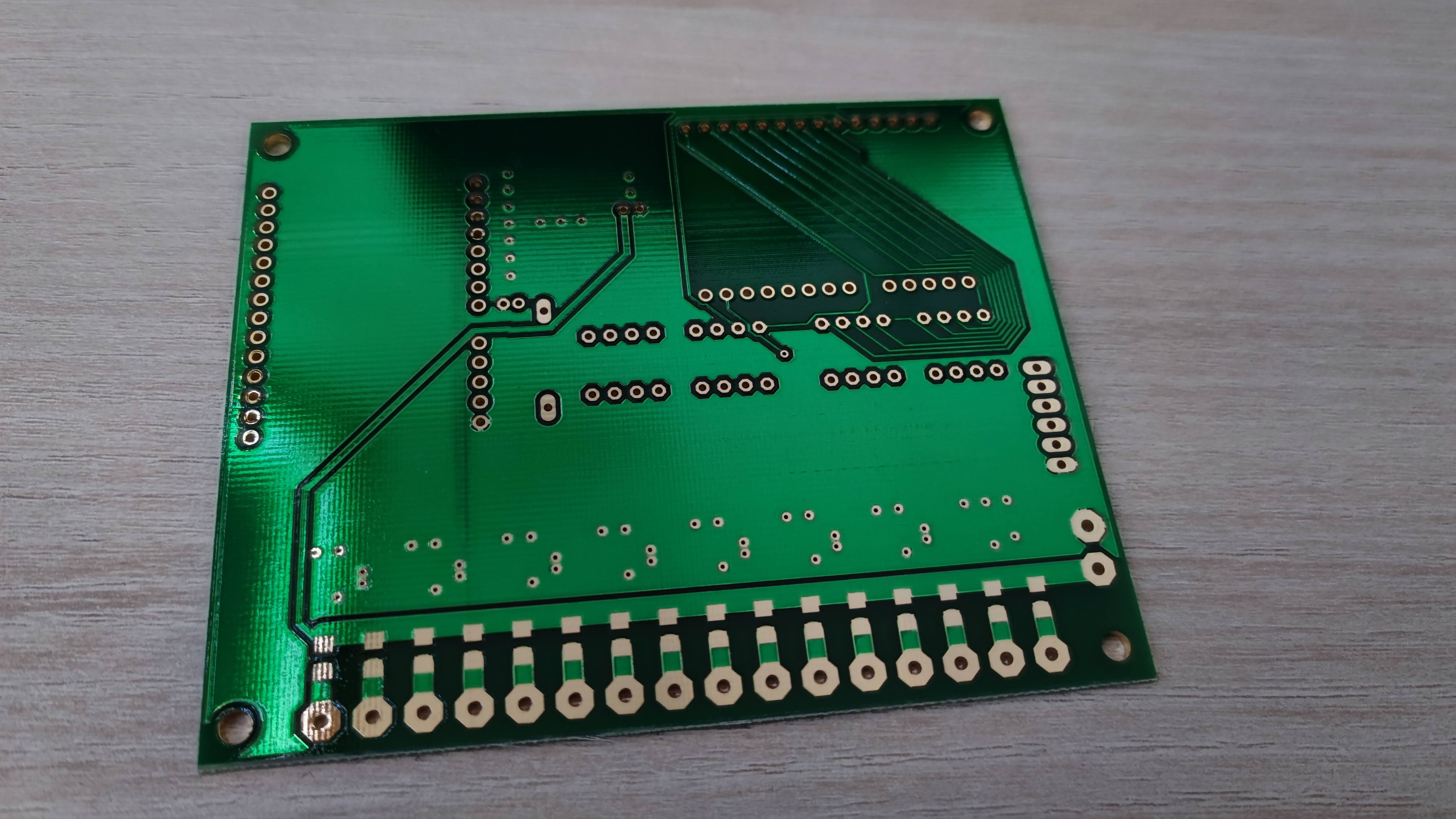
I will put sources on github when I have time and update this post with link, here are pictures of current design:
thanks for sharing your design. You’re right that TOWER needs more actor modules and we like your design.
Here are some top-of-my-head suggestions and questions:
I see lot of opportunities to make the PCB smaller. One idea is to use stack ability of Core and Battery Modules. If you put Core Module upside down on the PCB then you can also stack battery module and you don’t need to put battery footprint on your PCB. This might have disadvantage that the button and LED from Core Module might not be ideally visible. But the button could be connected to the BOOT pin on your PCB.
FET transistors does not have defined input state of their GATE input, when the Core Module will be flashed, empty and the GPIOs fill be floating (no logical 0 or 1 set) then GATE input can charge and open the FET, turn on LEDs. This can have issue in case you have lot of LEDs and the FET will be opened half-way, this will heat the FET a lot and can burn. Not necessarily needed to fix but just wanted to point that out.
That idea with Adafruit PWM module is clever. If I understand it right then you can use multiple PWM pcbs and Core Module will be only on the first one, other Adafruit PWM modules will have different I2C addres set. However this complicates design and population of that resitors. I would say that it would be possible to get rid of that through hole resistors and in case you use Adafruit PWM board, you can just use Core Module firmware which does not use those PWM GPIO pins and keep them floating. It might be better to put that module to your layout and see mechanically how it would work. You could also use this library to have it perfectly aligned https://www.diymodules.org/eagle-show-object?type=dm&file=diy-modules.lbr&device=PWM-SERVO-DRIVER-16CH
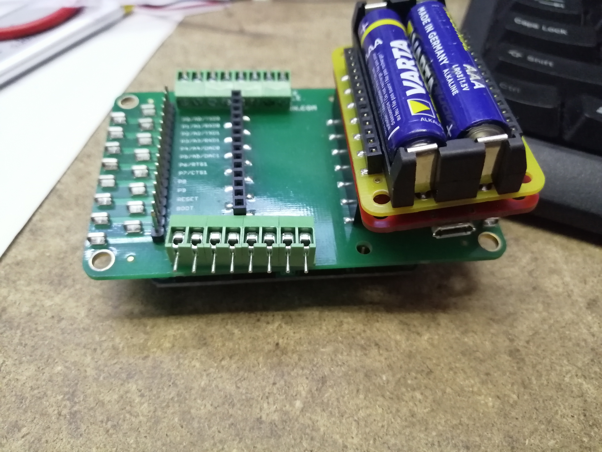
If Core Module is inserted in your PCB then the USB connector is not easily to be reached. There are capacitors and the battery module in the way.
It might not be necesarry to have those two FET disconnecting power. The diode might be enough. The improtant signal is BAT_OFF which disables battery module and that is all you need. Those disconnecting FETs would be necessary in case you can connect other module “from the bottom”. And since this module will not have pins from the bottom then you cannot connect any other power source (Power Module) that will need to react to VDD_OFF_IN signal. (please confirm @hubpav) image|255x125
It would be nice if I could have your eagle project to fiddle and try fit those parts differently to see where it could fit (not sure what pitch are the screw terminals etc…). I’m adding really rough hardware mock-up, there could be some issues.
But it might be possible to fit that PWM module on the bottom and at the same time have Core Module pins on the top, because that PWM module has space between pin headers of every 4 signals.
Let me know what do you think. We can arrange some videocall if you like. However we don’t want to discourage you with that suggestions above. It will work perfectly fine how you already designed it, but if you would like discuss this more or see areas where we could help you, let us know.
Hi Martin,
thanks a lot for feedback, I really appreciate it. Here are the eagle sources if you want to play with it: https://github.com/mixicz/harwario-board-pwm (I will eventually put there some OpenSCAD sources for parametric boxes as well)
Regarding your hints:
Yes, the board could be smaller and I did consider stacking battery and core modules (even having each of them on different side of PCB), but in my case total height was more important than PCB dimensions. I usually have it together in one box with slim 12/24V PSU (they are about 20 cm long while ≤ 25 mm in height), so there is not much gain squeezing it to smaller form. On the other hand, I tend to hide my creations in thin spaces (last one I had to squeeze in 32 mm wide space behind the cupboard). So my only limitation was 10×8 cm board size in free Eagle edition
Another disadvantage of stacking battery module on core is not being able to use P0 and P1 for PWM, as they are used by battery module. But it’s probably not that huge issue, as 7 remaining PWM outputs should be enough for most use cases and you can always use adafruit PWM module if you need more.
Good point, I think 10k pull down would do the trick and it will fit nicely in current board design.
Indeed it is possible to use multiple boards driven by single core module… it might be more convenient though to have extra header with I2C and power for this (I guess standard TOWER tag would do nicely and it might even be used for real tags). Regarding through hole resistors, I would like to keep them as they allow to connect core module signals to different outputs (not all core module outputs support PWM and THT resistors offsets for this fact).
USB connector orientation is really good point, I’d be up for quite a surprise if I’d had those manufactured. It will require significant rework of PCB though, but it’s quite important.
in your place, without my specific space restrictions, I would probably try to go with standard TOWER form 88×55 mm. With stacking battery on top of core, putting adafruit PWM module on other side of PCB and placing outputs on 2 sides, it should be possible.
Isn’t VDD_OFF_IN used to turn off power when core module is connected to USB?
Thanks a lot for helpful feedback. I don’t have much experience with HW design and I’m aware there is quite a room for improvement here. I certainly would not mind video call as it would help me to tune the design before I had the board manufactured
PS: If Hardwario would offer such universal boards, with pre-fitted PSU part and core module connector, I’d gladly grab few instead of creating my own
I also realized it would be good idea to be able to detect power outage, for example by optionally connecting BAT_OFF to some I/O pin (it doesn’t even have to be AD input, as we don’t need to measure voltage and simple on/off information should be enough).
Hi. Great to see another community HW design effort! I confirm VDD_OFF must be implemented only if multiple power sources come into play. If there is only one battery power source and one external power source, this task can be skipped. I suggest connecting BAT_OFF and external power input via a diode and series resistor as implemented e.g. in Battery Module.
Might be a bit off but we also have TOWER offering in Takachi enclosures. It can be combined with Maxi Base Module and soon CHESTER-A (we already have a few boards) which can be mounted in the top cover of Takachi. Just in case you would be interested to juggle with AC/DC converter (5V DC output) in an integrated housing.
So I took another look at core and power modules schematic and I think I do understand VDD_OFF handling now. If I’m wrong, please correct me.
each power source module (except battery) uses VDD_OFF_IN from bottom side, telling it to disconnect power as there is another active power source (logic “1” = disconnect power),
each power source module (except battery) provides VDD_OFF_OUT signal on top side of the module, indicating to other modules it does provide power.
Possible power source modules at this moment are power module and core module (when connected to USB). If stacked, lowest one takes priority, so when I put core module on top of power module, TOWER is powered from power module. If for some reason I put core module below power module, it will be powered from USB (speaking about 3.3V VDD).
So in my case, VDD_OFF_IN signal on core module is in fact VDD_OFF_OUT from my point of view, so I need to connect it to +3.3V (via diode and resistor), to tell the core module to disconnect it’s USB power. Otherwise it would remain connected potentially allowing reverse current into TLV73333 causing it to overheat (I guess voltage drop on diodes would prevent this, but it’s better to be safe).
As a side note, it might seem it is possible to stack multiple power sources with lowest active taking priority, but as there is no mechanism to pass through VDD_OFF signal in existing modules, it works safely with just 2 “power” modules (power module + core module with connected USB). Which is fine for 99.9% use cases I guess, but it’s useful to be aware of this when developing custom HW
Wow, your interpretation of power supply topology and logic is not only 100 % correct, but the way you have described it is worth copy&pasting to our docs I will speak to our devs to put it there if you don’t mind… Cheers!
Thanks to feedback from @hub.martin I have reworked the power supply to have capacitors as close as possible to step-down and used bigger inductor to be able to gracefuly handle power spikes from stepdown. I have also added ground plane as recommended in step-down application note, which also allowed to place more vias to outputs, potentially increasing max. current per output. And I moved away all components placed below the batery module, because it will sit very close to the board.
I kept the AP1501 step-down as I have few of them lying around, but in future revisions I will probably switch to some more optimal ones.
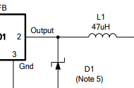
I would suggest to use shottky symbol for diodes in schematic, since your B340A diode is shottky. And also inductor symbol for L1. Current L1 symbol looks like some filter/ferrite bead for filtering.
One other thought - you have 390R resistors on FET gates. I’m not saying it is too much, but if you aim for higher PWM frequency then make sure the GATE signals are pretty sharp. Otherwise if they are too lienar, then the FEt transistor is just partially opened and there are more heat losses. I would put just few ohms resistor for EMI. It will also work perfectly fine with 0 ohm jumpers.
Regarding resistors, you are of course right (FET gate behaves like capacitor, so limiting current makes it charge/discharge more slowly). I used resistors primarily to allow routing signals to desired outputs, but didn’t realize at all, that using actual resistors may be contraproductive.
And regarding symbols, I’m aware of that. I was just too lazy going through eagle library looking for parts with proper package AND proper symbol
But as I’m actually making this public, I guess I should do it right, so I fixed it
Dry assembly shown some more problems. In particular, battery module header needs to be at least 5mm high, because:
C1 is too close to battery module header and is right under module,
R142+R162 have pads right under battery holder pin, which is too close.
Other issues I did encounter:
footprint of L1 is too small, I wasn’t able to find any which would fit,
signal paths are bit too thin to allow use of 70 µm Cu plating in company where they manufactured PCBs for me (they are 0.3 mm while thinnest recommended is 0.35 mm for 70 µm plating).
It is nothing that would prevent use of the PCB, but it is worth fixing in next version.
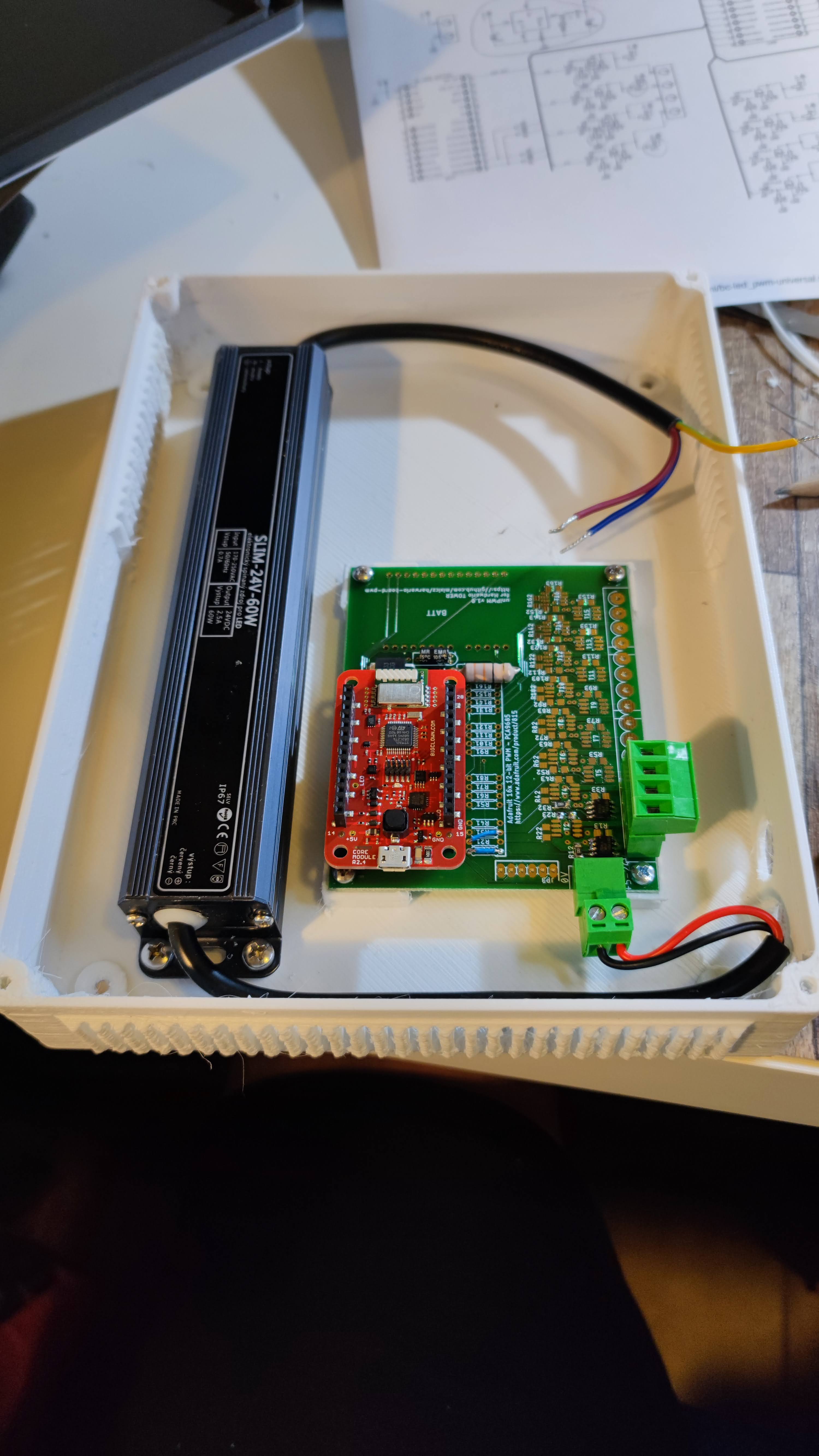
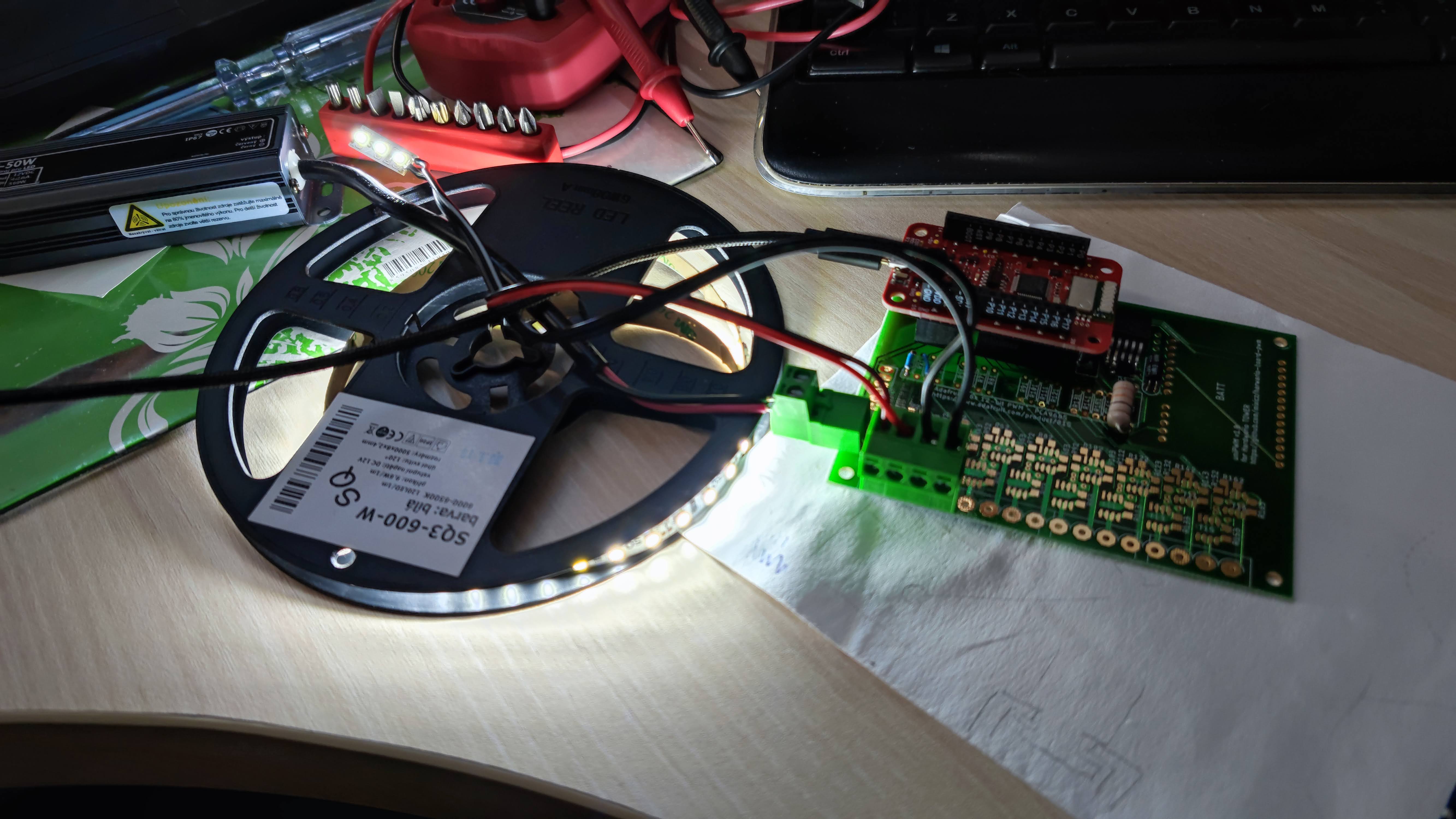
My first real use is for simple 2-channel PWM without battery backup. Please don’t mind ugly printed box, it was my first (and most probably last) attempt to print something from white FRjet filament. It is almost impossible to print any details (vent grills) or large surfaces with it. Black FRjet seems to use different flame retardant filling, making it much easier to print (it is still challenging though).
Congrats for your finished project and thanks for sharing!
Regarding the 70 um Cu plating - I wouldn’t bother to pay extra. The basic 35 um is enough for few centimetre traces. And your power traces from FET to the terminal block is thick enough (yes, you can do them even thicker if you want)


